Book a Reservation/Equipment Availability - Request Training

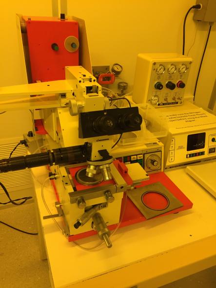
The Photolithography process transfers the patterned features from the mask on to the thin photoresist layer spin coated on silicon wafer. The Karl Suss MJB3 UV 400 mask aligner can provide a resolution down to 0.6 micrometer in optimal conditions. Considering the age of instrument, features size greater than 1 micrometer as reliably achieveable. Photoresist layer thickness can be varied from sub micrometer to more than 200 micrometer depending on the photoresist material, spin coating speed and other process conditions. Selected photoresists (S1805 and SU-8 2050) are sold by IMSE in small quantities.
IMSE Contact & Approved Trainer:
Rahul Gupta (rgupta24@wustl.edu)
Training Documents:
NOTE: User must demonstrate skills to IMSE staff before independent use.
Operating instructions
Recipe:
Click here to see existing recipes
Technical Info:
AZP4620 Resist datasheet
KL IR 15 Resist datasheet
S1805 Resist datasheet
SU8-2025 Resist datasheet
SU8-2050 Resist datasheet