Wet Etching
Wet etching is process of transferring pattering in top mask layer (e.g. Resist) to a second bottom layer (e.g. Silicon) using a selected wet solution (or wet etchant). Ideally, a selected wet etchant will not damage (or erode) top mask layer and only removes the material in second bottom layer. However, in actual process top mask layer is also etched. Wet etchant is selected to minimize etch rate (i.e. film thickness etched per unit time) of top mask layer and maximize the etch rate of second bottom layer.
Selectivity is often used to define the ratio of etch rates of two layers. Ideal wet etchant has selectivity >> 1.
Step-by-Step illustration of Wet Etching Process:

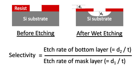
STEP 1a: Start with Si wafer (substrate) with Resist on top
STEP 1b: Cross-sectional view of Step 1a

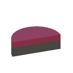
STEP 2a: Pattern photoresist using photolithography process (steps not shown)
STEP 2b: Cross-sectional view of Step 2a
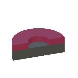
STEP 3a: After substrate is kept in chemical wet etch solution (not shown).
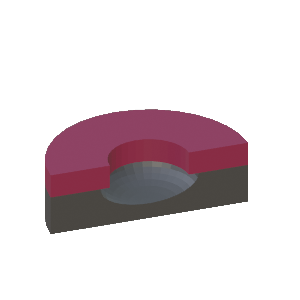
STEP 3b: Cross-sectional view of Step 3a
The above process can be carried out in IMSE Facility. IMSE offers dedicated Acid Fume Hood to accomplish the task safely. Click the link to start the training process.
Thin film metrology
Estimating etch peformance (etch rate, planar roughness, side wall roughness, etc.) is critical to fabricate device at micron scale in repeated manner. IMSE offers number of instruments ( Profilometer, Optical Microscope, Ellipsometer, SEM) to help in the quantitative measurements.
- Optical microscope can measure the critical dimension width. Qualitative images can help in determining whether film is completely removed.
- Profilometer can measure the thin film height as long as step edge is available in a patterned region. Instrument may also be used to estimate roughness of etched films.
- Ellipsometry can measure the film thickness of selected materials when deposited on Silicon substrate. Unlike profilometer, no patterned region should exist in the area of measurement.
Alternate to wet-etching Process:
The major disadvantage with wet-etching is the loss of critical dimensions due to isotropic nature of wet etching process. For example, 5 micron wide trench in resist may turn out to be 10 micron wide in etched layer underneath. As an alternate, Plasma based dry etching process is useful in preventing this loss of critical dimensions by keeping etching process anisotropic.