Spin Coating
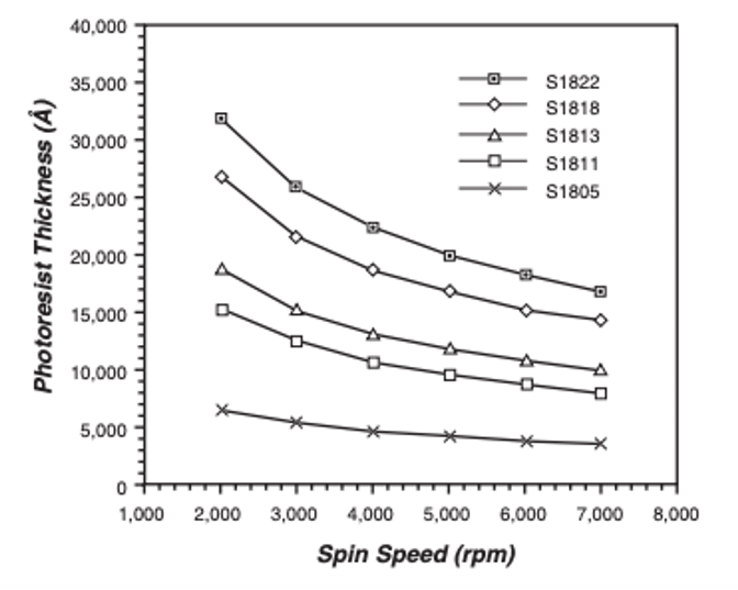
The process deposits thin film of organic material (typically photoresist) with desired film thickness on a Substrate. Substrate (or Silicon wafer) is spun at desired rotational speed (between 1000 rpm and 5000 rpm) for selected time (typically 45 sec). Spinning parameters are obtained from a data sheet supplied by manufacturer. An example Spin curve for S1805 Photoresist is shown below:
Step-by-Step illustration of Spin Coating Process:
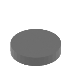
STEP 1: Start with Si wafer (substrate)
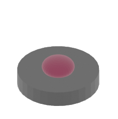
STEP 2: Drop few ml of resist on Si wafer
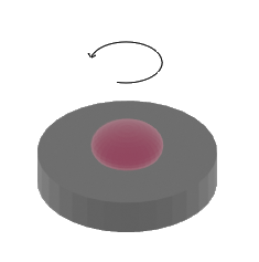
STEP 3: Rotate/Spin wafer at selected rpm

STEP 4: Obtain desired film thickness of resist on Si wafer
The above process can be carried out in IMSE Facility. Click here to learn more of our capability and start the training process.