Metal Deposition (E-beam)
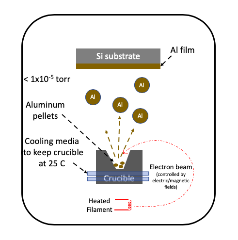
Metal Deposition by E-beam uses an electron beam to heat the material of interest and creates sufficient vapor pressure of the material in vacuum. E-beam is generated by thermionic emission (heating filament at high enough temperature to extract electrons) or field emission (using high electric field to extract electrons). E-beam is accelerated using controlled electric and magnetic field, and made to strike at the material of interest. Typically, the material is used in small pellet form (e.g. 1mm size) and kept inside/top of crucible (e.g. Boron Nitride ceramic). The crucible is kept at room temperature with water cooling underneath to prevent it from getting hot. The crucible material is selected such that it has a higher melting point and that does not form an alloy with material of interest. The evaporated material is then deposited on substrate of intereste. High mean free path in vacuum ensures that most evaporated material is deposited on the substrate of interest.
Comparision with Thermal Evaporation:
Thermal evaporation process heats the boat to a very high temperature, and hence the boat material can potentially contaminate the deposited film. However, in the E-beam deposition process, only the material of interest is heated. The boat is kept at room temperature at all times, and which gives a very high purity thin film. The E-beam technique can also deposit metals which may form alloys at high temperature with boat. For example, Platinum can be deposited by E-beam technique but not by Thermal evaporation.
Step-by-Step illustration of Metal Deposition Process:
STEP 1: Start with Si wafer (substrate)

STEP 2: Si wafer (substrate) with Aluminum thin film on top
The above process can be carried out in the IMSE Facility. IMSE offers AJA E-beam Evaporator to accomplish the task safely. Click the link to start the training process.
Thin film metrology
Estimating film deposition peformance (deposition rate, planar roughness, side wall roughness, etc.) is critical to fabricate a device at micron scale in repeated manner. IMSE offers a number of instruments ( Profilometer, Optical Microscope, In-situ Quartz Crystal Microbalance (QCM) Sensor, SEM) to help in the quantitative measurements.
- Optical microscope can measure the critical dimension width (for patterned thin films)
- Profilometer can measure the thin film height as long as a step edge is available. The simplest solution may be to cover part of planar surface with kapton tape during metal deposition. Instrument may also be used to estimate roughness of deposited films.
- In-situ QCM sensor can measure the thickness deposited on substrate in real-time. However, the sensor must be calibrated against another metrology (for example, Profilometer) before using it for measurement.