Chemical Vapor Deposition
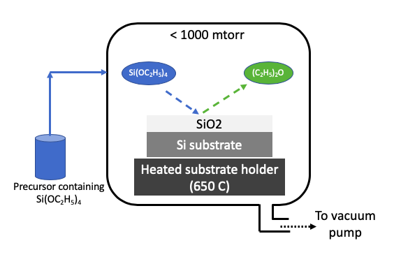
Chemical Vapor Deposition (CVD) uses one or more volatile precursors to deposit high quality thin films on desired substrates. Substrate is heated to desired temperature (650 C) to create chemical reaction from substrates. For example, Tetraethylorthosilicate precursor in vapor form will decompose at a high temperature on substrate to deposit Silicon Dioxide thin film. CVD process is carried out in vacuum to obtain uniform deposition and high purity films.
Many standard precursors are available today that can deposit metals, silicon oxide, silicon, silicon nitride, etc by CVD process. The precusor must be volatile, leave no impurity in deposited films, and give desired film properties (such as uniformity, electrical resistance, roughness, etc.). All byproducts from CVD surface reaction should be volatile and easily removable in vacuum. Precursors should not react among each other in vapor form, and only react at high temperature maintained at substrate.

The above process can be carried out in IMSE Facility. IMSE offers Nanofab PECVD system to accomplish the task safely. Click the link to start the training process.
Thin film metrology
Estimating film growth peformance (deposition rate, planar roughness, etc.) is critical to fabricate the device at micron scale in a repeated manner. IMSE offers a number of instruments ( Ellipsometer, Profilometer, Optical Microscope, SEM) to help in the quantitative measurements.
- Optical microscope can measure the critical dimension width (for patterned thin films)
- Profilometer can measure the thin film height as long as a step edge is available. The simplest solution may be to cover part of planar surface with kapton tape during metal deposition. Instrument may also be used to estimate roughness of etched films.
- Ellipsometry can measure the film thickness of selected materials when deposited on Silicon substrate. Unlike profilometer, no patterned region should exist in the area of measurement.
Graphene deposition
Graphene can de deposited on Cu thin substrate by flowing Methane and Hydrogen at high temperature (1200 C). Cu surface cleanliness is equally critical for deposition. Nanofab PECVD system at IMSE has established recipes to perform this sensitive process.