Photo Lithography
The process of photolithography uses photo light (UV light ~375nm wavelength) to pattern thin films of specialized organic materials (also known as photoresist or resist). Photoresist is a light sensitive material which changes in its chemical structure when exposed to UV light. Chemically modified photoresist is then removed in a chemical solution (also known as developer) to form a pattern of photoresist. Typically, a physical mask (also known as photomask) is used to control the exposed area of photoresist that sees a UV light.
Step-by-Step illustration of Photo Lithography Process:
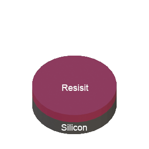
STEP 1: Start with Si wafer (substrate) with Resist on top
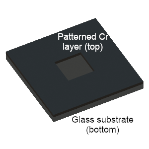
STEP 2: Purchase (or Fabricate) mask (Cr patterened on Glass)
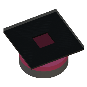
STEP 3: Flip mask and place on top of Resist coated Si. Typically, there is no separation between the two. Expose UV (~375nm) light above the glass mask (not shown in picture)
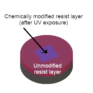
STEP 4: Part of the resist exposed to UV light is chemically modified (shown in darker color)
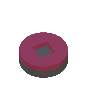
STEP 5(a): Substrate is kept in chemical solution (developer) (not shown). If chemically modified resist is removed after development, the process is called Positive lithography.
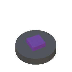
STEP 5(b): Substrate is kept in chemical solution (developer) (not shown). If chemically modified resist stays after development, the process is called Negative lithography.
The above process can be carried out in IMSE Facility. IMSE offer two Mask aligners: MJB Mask Aligner and KLOE Mask Aligner. Click the links to start the training process.
Alternate to mask based Photo Lithography Process:
UV laser (375nm) is another alternative to mask based UV lithography. Here, the UV laser is rastered on the resist coated substrate. UV laser motion (or areas exposed) is controlled by a design drawn in AutoCAD. Laser based exposure is often a slower photolithography process ( ~ hours) in comparison to mask based exposure (~ min). However, the UV laser provides the repeatability and feature capability down to 0.6 micro. Most applications of UV laser lithography include designing a one time photomask (Resist/Cr/Glass) or writing features with size below 1 micro. IMSE offers the Heidelberg UV Laser Writer to accomplish this process. Click the link to learn more and start the training process.
Additional Links
How Negative lithography works?