Reactive Ion Etching (Dry etching)
Reactive Ion etching (RIE) is the process of transferring pattering in a top mask layer (e.g. Resist) to a second bottom layer (e.g. Silicon) using a plasma of etching gases (e.g. CF4 gas). Plasma is formed when a high electric field breaks down the gas molecules to ions, neutral, and radicals. Typically, an electric field is directly applied to a substrate or wafer. These species are highly reactive and can etch thin film material in both chemical form or physical (sputtering) form. Chemical based etching occurs when reactant species (e.g. Fluorine radicals) react with material (e.g. Silicon) to form a byproduct (e.g. SiFx) which is volatile at room temperature and low pressure (~10 mtorr). Physical etching occurs when plasma ions are propelled under an electric field to strike thin film material at high velocity. In most cases, the combination of chemical and physical forms gives synergistics benefits in etch performance. For example, an etching profile can be anisotropic, or higher etch rates can be obtained for the same selectivity.
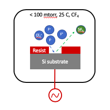
Since there is not a wet chemical in the RIE process, etching is sometimes referred to as Dry etching. Other synonyms of the process include - Plasma etching. Most advanced RIE systems come with dual plasma sources to achieve better control over the etch rate, selectivity and side wall angle. For example, IMSE RIE etching uses an Inductively Coupled Plasma (ICP) source on the top part of the chamber and a second Plasma source on the wafer. This configuration is often called ICP/RIE etching.
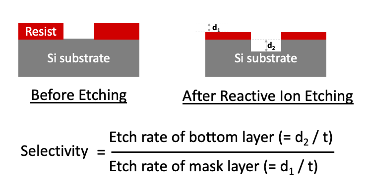
Ideally, a selected RIE etch process/chemistry will not damage (or erode) the top mask layer and will only remove the material in the second bottom layer. However, in the actual process the top mask layer is also etched. Plasma chemistry is selected to minimize the etch rate (i.e. film thickness etched per unit time) of the top mask layer and maximize the etch rate of the second bottom layer.
Selectivity is often used to define the ratio of etch rates of the two layers. Ideal Plasma etch conditions has a selectivity >> 1.
Step-by-Step illustration of Wet Etching Process:

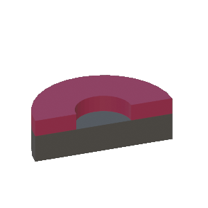
STEP 1a: Start with Si wafer (substrate) with Resist on top
STEP 1b: Cross-sectional view of Step 1a
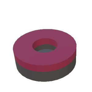
STEP 2a: Pattern photoresist using photolithography process (steps not shown)
STEP 2b: Cross-sectional view of Step 2a
STEP 3a: After substrate is etched in RIE etcher (not shown).
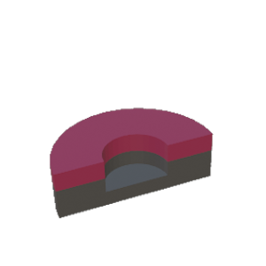
STEP 3b: Cross-sectional view of Step 3a
The above process can be carried out in the IMSE Facility. IMSE offers the Oxford RIE etcher to accomplish the task safely. Click the link to start the training process.
Thin film metrology
Estimating etch performance (etch rate, planar roughness, side wall roughness, etc.) is critical to fabricating devices at the micron scale in a repeated manner. IMSE offers a number of instruments ( Profilometer, Optical Microscope, Ellipsometer, SEM) to help in the quantitative measurements.
- Optical microscopes can measure the critical dimension width. Qualitative images can help in determining whether the film is completely removed.
- Profilometers can measure the height of thin film as long as a step edge is available in a patterned region. The instrument may also be used to estimate the roughness of etched films.
- Ellipsometer can measure the film thickness of selected materials when deposited on Silicon substrate. Unlike a profilometer, no patterned region should exist in the area of measurement.
Limitations of RIE Process:
Certain materials (such as Gold) do not form etch byproducts with sufficient vapor pressure, and hence do not etch easily. Metal etch processes can also leave residue in parts of the etching chamber. These residues can cause yield issues when etching other materials (such as SiO2). For these reasons, the IMSE limits metals that can be etched or used as a mask in the Oxford RIE instrument.
Deep Si RIE etch (cyclic) process
Continuous RIE process as explained above are typically used to etch thin films with thickness less than 50 microns. As films are etched deeper, it becomes difficult to maintain high selectivity and vertical sidewalls in patterned structures. The Deep RIE process overcomes this limitation by using a two-step cyclic process where one step is used to deposit thin polymer film (using C4F8 gas) and a second step is used to remove the polymer (using SF6 gas) at bottom of etched structure. A pair of two steps constitues 1 cycle and is repeated (or number of cycles) to get the desired etch depth. Repeated processes leads to additional roughness on the sidewalls. These are also called as scallops.
Typically, this process is used to partially etch Si substrate with thickness > 100 um, and sometimes to completely etch a hole (or feature) in Si substrate. Other synonymous names of Deep Si etch include Bosch etch, Deep etch, Bosch RIE.
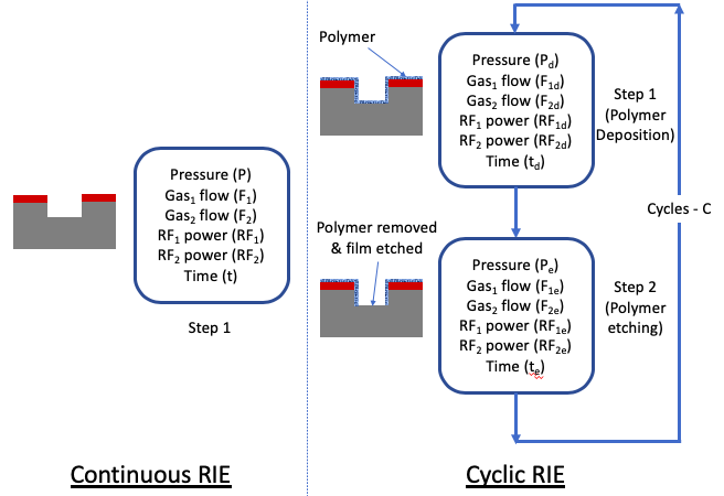
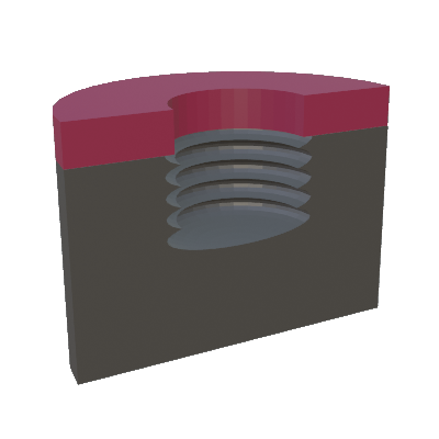
Formation of scallops during Deep Si RIE process