Metal Patterning
Metal Patterning is a process of patterning thin metal films using a combination of metal deposition, metal removal, and photolithography. The two widely used methods are:
- Subtractive Transfer - Resist layer is patterned on top of metal thin film. Exposed metal film is then etched with wet etchant, and followed by removal of resist to give a patterned metal layer.
- Additive Transfer (lift-off method) - Metal is deposited over patterned resist layer. Resist layer is then removed (or lifted off) to give patterned metal layer. Single layer of resist may be replaced with two layers of resist for better repeatability of lift-off process.
The above process can be carried out in IMSE Facility. IMSE offers Fume hoods, Lithography and Metal deposition instruments to accomplish the task safely. Click the link to start the training process.
Step-by-Step illustration of Metal Deposition using Subtractive Transfer Process:
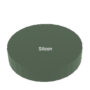
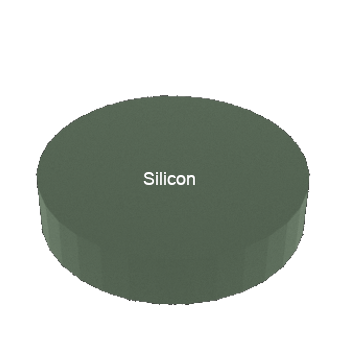
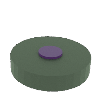
STEP 1: Start with Si wafer (substrate)
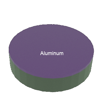
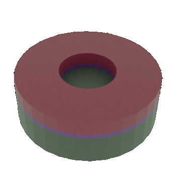
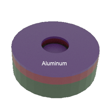
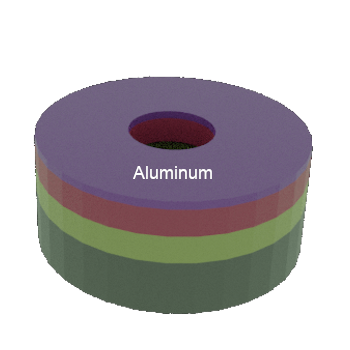
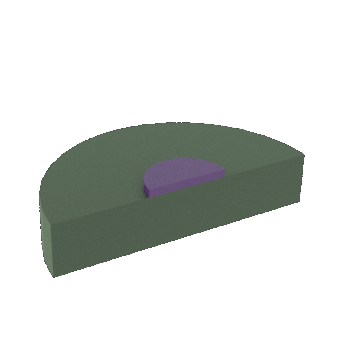
STEP 2: Si wafer (substrate) with Aluminum thin film on top
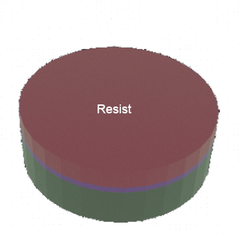
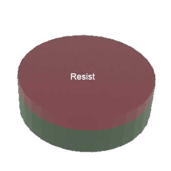
STEP 3: Al/Si wafer (substrate) with Resist thin film on top
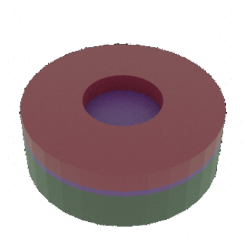
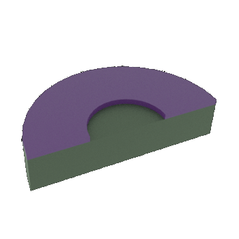
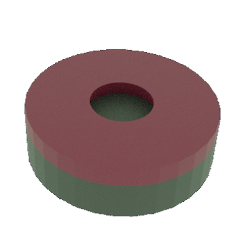
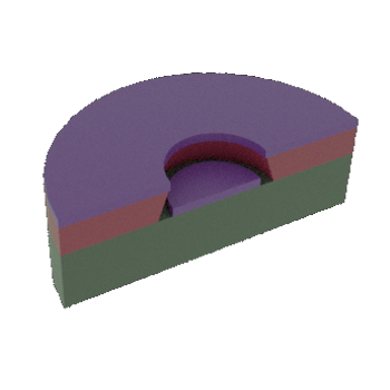
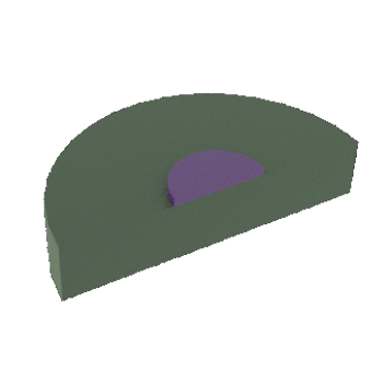
STEP 4a: Al/Si wafer (substrate) with patterned Resist thin film on top (lithography steps not shown)
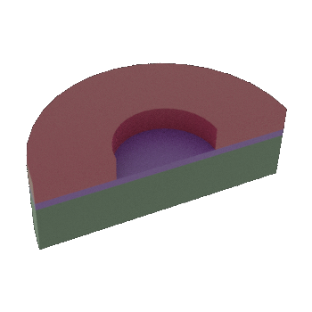
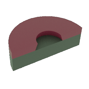
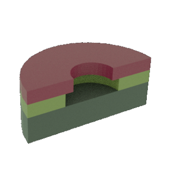
STEP 4b: Cross-sectional view of 4a
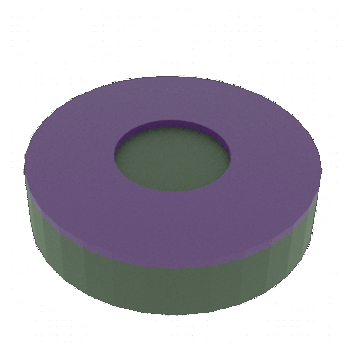
STEP 5a: Exposed Al removed by Wet etching
STEP 5b: Cross-sectional view of 5a (Undercut in Al layer not shown)
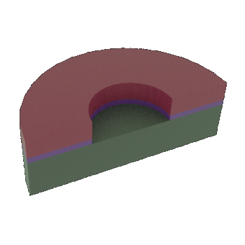
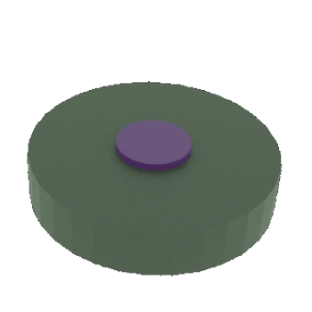
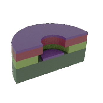
STEP 6a: Patterned metal layer after Resist layer is removed
STEP 6b: Cross-sectional view of 6a
Step-by-Step illustration of Metal Deposition using Additive Transfer Process with Single layer resist:
Typically, the resist selected is negative resist to give a negative profile which helps in lift-off process.
STEP 1: Start with Si wafer (substrate)
STEP 2: Si wafer (substrate) with two layers of resist on top
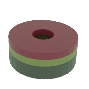
STEP 3a: Patterned (both) Resist layer on top (lithography steps not shown)
STEP 3b: Cross-sectional view of 3a (NOTE: Undercut in LOR-10B layer depends on development time)
STEP 4a: After aluminum metal deposition (equipment steps not shownn)
STEP 4b: Cross-sectional view of 4a
STEP 5a: Patterned metal layer after Resist layer is lift-off in wet solution
STEP 5b: Cross-sectional view of 5a
Step-by-Step illustration of Metal Deposition using Additive Transfer Process with two layer resist:
In two layer process, first resist layer is LOR-10B and second layer is positive (or negative) resist. Developer solution used for second layer resist also removes exposed LOR-10B layer.
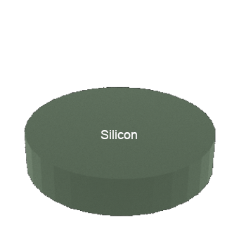
STEP 1: Start with Si wafer (substrate)
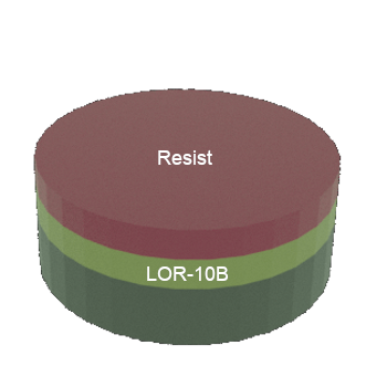
STEP 2: Si wafer (substrate) with single layer of resist on top
STEP 3a: Patterned Resist layer on top (lithography steps not shown)
STEP 3b: Cross-sectional view of 3a
STEP 4a: After aluminum metal deposition (equipment steps not shownn)
STEP 4b: Cross-sectional view of 4a (NOTE: Negative profile in resist layer)
STEP 5a: Patterned metal layer after Resist layer is lift-off in wet solution
STEP 5b: Cross-sectional view of 5a
Thin film metrology
Estimating metal pattern peformance (critical dimensions change, feature widths, planar roughness, side wall roughness, etc.) is critical to fabricate device at micron scale in repeated manner. IMSE offers number of instruments (Profilometer, Optical Microscope, SEM) to help in the quantitative measurements.
- Optical microscope can measure the critical dimension width (for patterned thin films)
- Profilometer can measure the thin film height as long as step edge is available. Instrument may also be used to estimate roughness of etched films.