Atomic Layer Deposition (ALD)
Atomic Layer Deposition (ALD) uses one or more volatile precursors or gases to deposit high quality thin films on desired substrates with precision controlled at angstrom length scale. Unlike a CVD process which uses continuous flow of gases, the ALD process introduces precursors in the chamber in a sequential manner. Sequential approach and chemistry selection ensures that each precursor only forms a single monolayer at a time. For example, Al2O3 is deposition by first flowing Trimethyl aluminum precursor, then purging chamber with nitrogen, then flowing water vapor as second precursor, and then purging with nitrogen again. These four steps constitute 1 ALD cycles, and gives a growth rate of ~1 Angstron per cycle. A cycle is repeated to get the desired film thickness. Nitrogen purge between the steps of ALD cycle prevents an undesired reaction in vapor phase. The ALD process can deposit films in a highly uniform manner in any size or shape especially when repeatability is critical at angstrom length scale. ALD precursors are carefully selected to foster desired ALD chemistry on heated substrate. Substrate is typically heated to a desired temperature (100 - 350 C) to create chemical reaction on substrates. ALD process is carried out in vacuum to obtain uniform deposition and high purity films.
Many standard precursors are available today that can deposit metals, metal oxides, silicon oxide, etc by ALD process. The precusor must be volatile, leave no impurity in deposited films, and give desired film properties (such as uniformity, electrical resistance, roughness, etc.). All byproducts from ALD surface reaction should be volatile and easily removable in vacuum. Precursors should not react among each other in vapor form, and only react at high temperature maintained at substrate.
The above process can be carried out in IMSE Facility. IMSE offers ALD Instrument to accomplish the task safely. Click the link to start the training process.
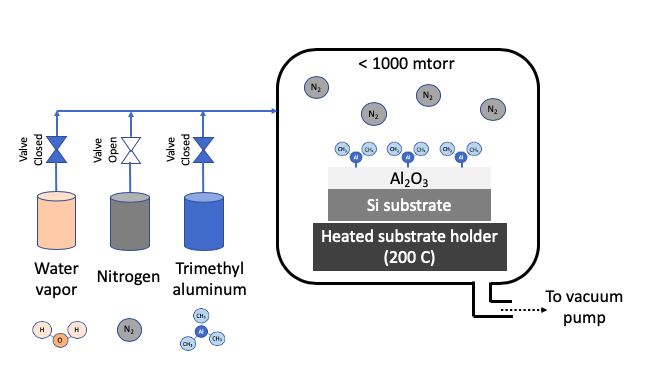
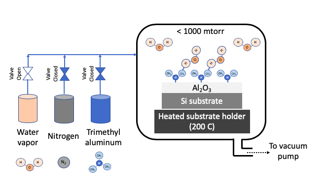
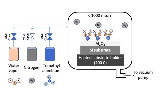
Step-by-Step illustration of steps in 1 ALD Cycle:

STEP 1: Passivate surface with Precursor 1 (Trimethyl aluminum)

STEP 2: Remove excess Precursor 1 with Nitrogen purge

STEP 3: Introduce Precursor 2 (water vapor) to complete surface reaction

STEP 4: Remove excess Precursor 2 with Nitrogen purge
Thin film metrology
Estimating film growth peformance (deposition rate, planar roughness, etc.) is critical to fabricate the device at micron scale in a repeated manner. IMSE offers a number of instruments ( Ellipsometer, Profilometer, Optical Microscope, SEM) to help in the quantitative measurements.
- Optical microscope can measure the critical dimension width (for patterned thin films)
- Profilometer can measure the thin film height as long as step edge is available. The simplest solution may be to cover part of planar surface with kapton tape during metal deposition. Instrument may also be used to estimate roughness of etched films.
- Ellipsometry can measure the film thickness of selected materials when deposited on Silicon substrate. Unlike a profilometer, no patterned region should exist in the area of measurement.