Metal Deposition (Sputtering)
Metal Deposition by Sputtering starts with creating high electrical field around source material (or target) of interest. Electrical field creates Plasma and removes material atoms from the source material. These removed material is then deposited on substrate of interested. High mean free path in vaccum ensures that most sputtered (or removed material) is deposited on the substrate of interest.
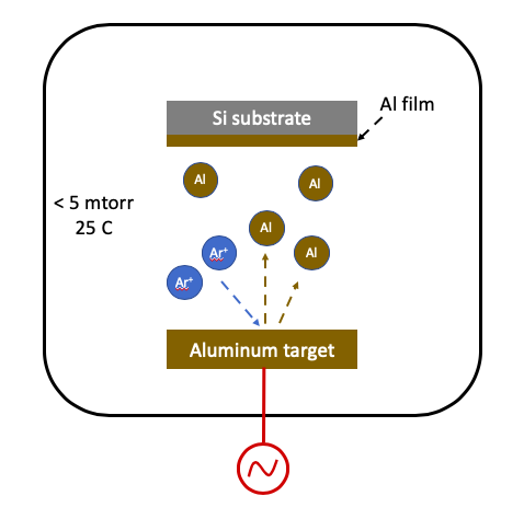
Plasma source can be either RF or DC. Typically, DC source is used for metal (or electrically conducting) source (or target) material, and RF source is used for insulator source (or target) materials. Ar is primarily the source gas as it is easy to ionize and create plasma. For certain use cases, oxygen can be mixed with Ar to deposit oxide forms on metal source.
Step-by-Step illustration of Metal Deposition Process:
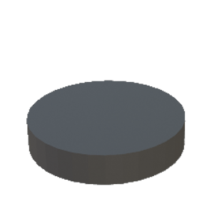
STEP 1: Start with Si wafer (substrate)
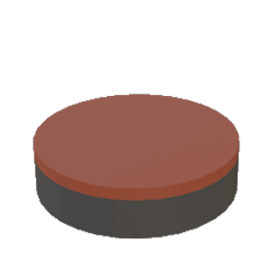
STEP 2: Si wafer (substrate) with Aluminum thin film on top
The above process can be carried out in IMSE Facility. IMSE offers Sputter Deposition Tool to accomplish the task safely. Click the link to start the training process.
Thin film metrology
Estimating film deposition peformance (deposition rate, planar roughness, side wall roughness, etc.) is critical to fabricate device at micron scale in repeated manner. IMSE offers number of instruments ( Profilometer, Optical Microscope, In-situ Quartz Crystal Microbalance (QCM) Sensor, SEM) to help in the quantitative measurements.
- Optical microscope can measure the critical dimension width (for patterned thin films)
- Profilometer can measure the thin film height as long as step edge is available. The simplest solution may be to cover part of planar surface with kapton tape during metal deposition. Instrument may also be used to estimate roughness of deposited films.
- In-situ QCM sensor can measure the thickness deposited on substrate in real-time. However, the sensor must be calibrated against another metrology (for example, Profilometer) before using for measurement.